KiCad EDA is a Cross Platform and Open Source Electronics Design Automation Suite
PCB Layout
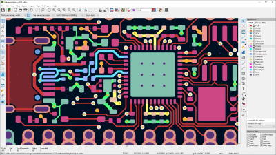
Make professional PCB layouts with up to 32 copper layers. KiCad now has a push-and-shove router that is capable of routing differential pairs and interactively tuning trace lengths.
Schematic Capture
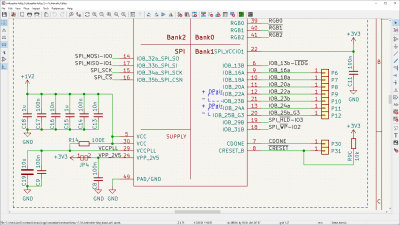
KiCad's Schematic Editor supports everything from the most basic schematic to a complex hierarchical design with hundreds of sheets. Create your own custom symbols or use some of the thousands found in the official KiCad library. Verify your design with an integrated SPICE simulator and electrical rules checker.
3D Viewer
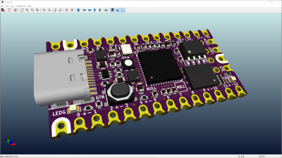
KiCad includes a 3D viewer that you can use to inspect your design in an interactive canvas. You can rotate and pan around to inspect details that are difficult to inspect on a 2D view. Multiple rendering options allow you to modify the aesthetic appearance of the board or to hide and show features for easier inspection.
KiCad is an open-source project, download instructions above are provided by the community.